- 您现在的位置:买卖IC网 > Sheet目录336 > LC4064ZC-EV (Lattice Semiconductor Corporation)BOARD EVAL FOR ISPMACH 4064ZC
�� �
�
�Lattice� Semiconductor�
�ispMACH� 4000V/B/C/Z� Family� Data� Sheet�
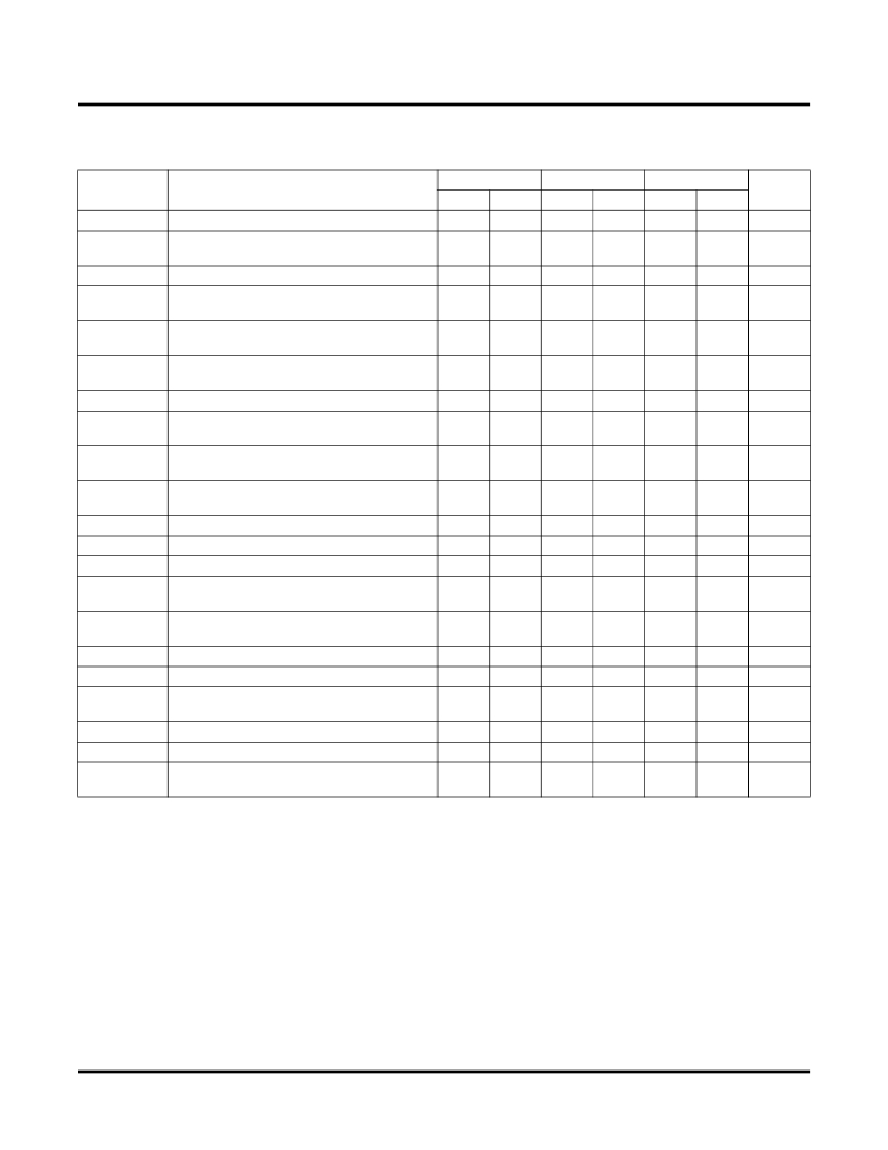
�ispMACH� 4000Z� External� Switching� Characteristics�
�Over� Recommended� Operating� Conditions�
�-35�
�-37�
�-42�
�f� MAX�
�Parameter�
�t� PD�
�t� PD_MC�
�t� S�
�t� ST�
�t� SIR�
�t� SIRZ�
�t� H�
�t� HT�
�t� HIR�
�t� HIRZ�
�t� CO�
�t� R�
�t� RW�
�t� PTOE/DIS�
�t� GPTOE/DIS�
�t� GOE/DIS�
�t� CW�
�t� GW�
�t� WIR�
�4�
�f� MAX� (Ext.)�
�Description� 1,� 2,� 3�
�5-PT� bypass� combinatorial� propagation� delay�
�20-PT� combinatorial� propagation� delay�
�through� macrocell�
�GLB� register� setup� time� before� clock�
�GLB� register� setup� time� before� clock� with�
�T-type� register�
�GLB� register� setup� time� before� clock,� input�
�register� path�
�GLB� register� setup� time� before� clock� with� zero�
�hold�
�GLB� register� hold� time� after� clock�
�GLB� register� hold� time� after� clock� with� T-type�
�register�
�GLB� register� hold� time� after� clock,� input�
�register� path�
�GLB� register� hold� time� after� clock,� input�
�register� path� with� zero� hold�
�GLB� register� clock-to-output� delay�
�External� reset� pin� to� output� delay�
�External� reset� pulse� duration�
�Input� to� output� local� product� term� output�
�enable/disable�
�Input� to� output� global� product� term� output�
�enable/disable�
�Global� OE� input� to� output� enable/disable�
�Global� clock� width,� high� or� low�
�Global� gate� width� low� (for� low� transparent)� or�
�high� (for� high� transparent)�
�Input� register� clock� width,� high� or� low�
�Clock� frequency� with� internal� feedback�
�clock� frequency� with� external� feedback,�
�[1� /� (t� S� +� t� CO� )]�
�Min.�
�—�
�—�
�2.2�
�2.4�
�1.0�
�2.0�
�0.0�
�0.0�
�1.0�
�0.0�
�—�
�—�
�1.5�
�—�
�—�
�—�
�1.0�
�1.0�
�1.0�
�—�
�—�
�Max.�
�3.5�
�4.4�
�—�
�—�
�—�
�—�
�—�
�—�
�—�
�—�
�3.0�
�5.0�
�—�
�7.0�
�6.5�
�4.5�
�—�
�—�
�—�
�267�
�192�
�Min.�
�—�
�—�
�2.5�
�2.7�
�1.1�
�2.1�
�0.0�
�0.0�
�1.0�
�0.0�
�—�
�—�
�1.7�
�—�
�—�
�—�
�1.5�
�1.5�
�1.5�
�—�
�—�
�Max.�
�3.7�
�4.7�
�—�
�—�
�—�
�—�
�—�
�—�
�—�
�—�
�3.2�
�6.0�
�—�
�8.0�
�7.0�
�4.5�
�—�
�—�
�—�
�250�
�175�
�Min.�
�—�
�—�
�2.7�
�2.9�
�1.3�
�2.6�
�0.0�
�0.0�
�1.3�
�0.0�
�—�
�—�
�2.0�
�—�
�—�
�—�
�1.8�
�1.8�
�1.8�
�—�
�—�
�Max.�
�4.2�
�5.7�
�—�
�—�
�—�
�—�
�—�
�—�
�—�
�—�
�3.5�
�7.3�
�—�
�8.0�
�8.0�
�4.8�
�—�
�—�
�—�
�220�
�161�
�Units�
�ns�
�ns�
�ns�
�ns�
�ns�
�ns�
�ns�
�ns�
�ns�
�ns�
�ns�
�ns�
�ns�
�ns�
�ns�
�ns�
�ns�
�ns�
�ns�
�MHz�
�MHz�
�1.� Timing� numbers� are� based� on� default� LVCMOS� 1.8� I/O� buffers.� Use� timing� adjusters� provided� to� calculate� other� standards.�
�2.� Measured� using� standard� switching� GRP� loading� of� 1� and� 1� output� switching.�
�3.� Pulse� widths� and� clock� widths� less� than� minimum� will� cause� unknown� behavior.�
�4.� Standard� 16-bit� counter� using� GRP� feedback.�
�24�
�Timing� v.2.2�
�发布紧急采购,3分钟左右您将得到回复。
相关PDF资料
LCMXO2280C-C-EVN
BOARD CONTROL EVAL MACHXO
LDB100-024SW
LED POWER SUPPLY 24V 0-4A 100W
LDB150-048SW
LED POWER SUPPLY 24V-48V 3.125A
LDB200-048SW
LED POWER SUPPLY 24V-48V 4.2A
LDB75-048SW
LED POWER SUPPLY 24V-48V 1.56A
LDS8141-002-T2
IC LED DRIVER WHIT BCKLGT 16WQFN
LDS8160-002-T2
IC LED DVR WHT/RGB BCKLGT 16WQFN
LDS8620-002-T2
IC LED DRIVER FLASH 16WQFN
相关代理商/技术参数
LC4064ZE4MN100C
制造商:LATTICE 制造商全称:Lattice Semiconductor 功能描述:1.8V In-System Programmable Ultra Low Power PLDs
LC4064ZE4MN100CES
制造商:LATTICE 制造商全称:Lattice Semiconductor 功能描述:1.8V In-System Programmable Ultra Low Power PLDs
LC4064ZE4MN100I
制造商:LATTICE 制造商全称:Lattice Semiconductor 功能描述:1.8V In-System Programmable Ultra Low Power PLDs
LC4064ZE4MN100IES
制造商:LATTICE 制造商全称:Lattice Semiconductor 功能描述:1.8V In-System Programmable Ultra Low Power PLDs
LC4064ZE4MN144C
制造商:LATTICE 制造商全称:Lattice Semiconductor 功能描述:1.8V In-System Programmable Ultra Low Power PLDs
LC4064ZE-4MN144C
功能描述:CPLD - 复杂可编程逻辑器件 64MC 64 I/O Ultra Low Power 1.8V
RoHS:否 制造商:Lattice 系列: 存储类型:EEPROM 大电池数量:128 最大工作频率:333 MHz 延迟时间:2.7 ns 可编程输入/输出端数量:64 工作电源电压:3.3 V 最大工作温度:+ 90 C 最小工作温度:0 C 封装 / 箱体:TQFP-100
LC4064ZE4MN144CES
制造商:LATTICE 制造商全称:Lattice Semiconductor 功能描述:1.8V In-System Programmable Ultra Low Power PLDs
LC4064ZE4MN144I
制造商:LATTICE 制造商全称:Lattice Semiconductor 功能描述:1.8V In-System Programmable Ultra Low Power PLDs